On June 2, 2005, Carl Zeiss SMT AG announced that it had agreed to acquire Nawotec GmbH, a Rossdorf, Germany-based supplier of semiconductor photomask-repair equipment. ZEISS said the deal would strengthen its nanostructuring and mask-repair capabilities; the transaction was expected to close in the second quarter of 2005, but the available announcement does not confirm that it did. The purchase price was not reported. EE Times reported the announcement.
What ZEISS announced
The transaction concerned Nawotec, also styled NaWoTec, and Carl Zeiss SMT AG, ZEISS’s semiconductor business. The companies had collaborated on a photomask-repair tool before the announcement. ZEISS was based in Oberkochen, Germany; Nawotec was based in Rossdorf.
The distinction between an announced deal and a confirmed closing matters: the June 2 report says completion was expected during Q2 2005, but does not provide a later closing confirmation. It also gives no purchase price or transaction structure.
What Nawotec’s technology did
A photomask, or reticle, carries a pattern used in semiconductor lithography to form features on wafers. A defect on a mask can be reproduced across many chips, so inspecting and correcting masks can protect valuable production material and avoid discarding a mask that can be repaired.
Crashes, No Sound, or Screen Glitches?
Random freezes, missing sound and display glitches usually trace back to one bad driver. Find and replace yours safely.Free scan · under a minutePC Slower Than It Used to Be?
A free scan shows the junk files, broken settings and background clutter dragging Windows down - then fixes them in one click.Free scan · Windows 10 & 11#1 Best Overall
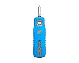
- HIGH-RESOLUTION IMAGING: Provides crystal-clear 200x magnification images of fiber optic connector ferrules in real-time on your mobile device or tablet.
- ONE PRESS AUTO ANALYSIS: Automatically generates and records a Pass/Fail report with just a single press.
- VERSATILE COMPATIBILITY: Inspects male and female PC/UPC SC, ST, FC, and LC fiber connectors and ports with the 5 included adapters.
- FREE APP & CROSS-PLATFORM: Download the app for free on Android and iOS devices for easy connectivity and viewing.
- USB CONNECTIVITY: Can also connect via USB to OTDR-1500 or other compatible devices for additional functionality.
Nawotec had developed an electron-beam photomask-repair tool in cooperation with ZEISS. The 2005 report describes a technology portfolio combining mask-repair process know-how, adaptable application software, computer-controlled gas-injection hardware for carefully controlled chemical reactions, and nanostructuring expertise. It does not provide a product model, detailed specifications, or evidence of commercial shipments beyond a beta system.
Why mask repair mattered to advanced lithography
As lithography pursued smaller features, mask defects became more consequential. EUV development also brought requirements for mask inspection, correction, and process control. Electron-beam repair was one emerging approach alongside established focused-ion-beam and laser-based systems, with nanomachining also part of the developing toolkit, according to the contemporaneous EE Times account.
These approaches are not interchangeable by definition, and the available report does not compare their performance or specify which defect classes Nawotec’s tool could handle. The strategic point is narrower: repair equipment addressed a supporting step in the lithography workflow, not the wafer exposure performed by a lithography scanner.
Rank #2

- Visually check tire tread depth on driver and steer tires
- Quickly inspect brake stroke to determine compliance
- Go-No-Go Gauge for brake lining thickness
- Find windscreen chips and cracks that are to large
How the deal fit ZEISS’s semiconductor strategy
ZEISS was already known in semiconductor manufacturing for lithography optics. The Nawotec announcement pointed to an effort to add process and equipment capabilities around nanostructuring and mask repair, extending its involvement into another part of the manufacturing chain rather than simply adding an optical component business.
ZEISS’s later semiconductor-business description includes lithography optics, photomask systems, and process-control solutions, providing context for the broader scope of its activities. That later portfolio does not, by itself, establish what Nawotec contributed commercially after 2005. See ZEISS’s 2024 semiconductor-business announcement.
What the report said about Intel
EE Times reported that Intel received the first beta version of Nawotec’s tool and was reportedly using it to inspect masks in an EUV pilot line. The distinction is important: the tool was a mask-repair system, while the reported use involved mask inspection in an EUV development setting; it was not an EUV lithography machine. Intel Capital was also named among Nawotec’s investors. These are claims attributed to the 2005 industry report, not independently verified current facts.
Rank #3
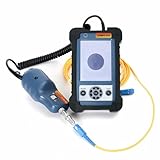
- 400× Magnification Ability,less more 1um Resolution.
- 3.5 Inch Monitor support in Video record/Voice editing/Image Capture/Zoom out &in function/File Generated &Stored/Grid Judgment.
- 27 assorted of tips available to have both PC end face inspection.
- 60°angle tips to test multiple types of connectors in many hard-to-access places or bottom of patch panel.
- Ability to inspect multiple cores end face
The competitive landscape in 2005
The report described photomask repair as a difficult market, with many vendors competing for relatively limited spending. It referenced FEI Co., SII NanoTechnology, and Rave LLC, as well as focused-ion-beam, laser, electron-beam, and nanomachining approaches. This is a snapshot of the market as reported in 2005, not a guide to current suppliers or company ownership.
What remains undisclosed
- The purchase price and transaction structure.
- A later confirmation that the announced acquisition closed.
- Nawotec’s founding date, workforce, product specifications, or detailed commercial record.
- How the company or its technology developed inside ZEISS after the announcement.
The 2005 report named Wellington Partners, CIPIO, Target Partners, and Intel Capital as Nawotec investors, but did not state their stake sizes, board roles, or whether each investor exited through the transaction. EE Times’s account is the source for these transaction and investor details.
Do these 3 things before closing this tab:
1Repair Windows errors before they cause bigger problems2Fix the driver behind crashes, sound loss and screen glitches3Clear out junk files and repair common Windows errorsThis historical deal should not be confused with later ZEISS acquisitions in unrelated businesses, including its 2025 acquisition of Pi Imaging Technology and its 2026 acquisition of selected Vivior assets: ZEISS on Pi Imaging and ZEISS on Vivior.
Quick Recap
Product prices and availability are accurate as of the date/time indicated and are subject to change. Any price and availability information displayed on Amazon at the time of purchase will apply.




