The Tool Desk
Outbyte PC Repair FREEClear out junk files and repair common Windows errorsFree Scan →Outbyte Driver Updater FREEScan for outdated or missing drivers - takes under a minuteDriver Scan →ASML’s sales and profit are rising because customers are investing in the advanced logic and memory chips needed for AI—and those chips require more lithography capacity. ASML reported €32.7 billion in 2025 net sales and €9.6 billion in net income. In the second quarter of 2026, it reported €9.3 billion in sales and €2.9 billion in net income, then raised its full-year sales outlook to €43–45 billion. The results show how AI investment can flow through the semiconductor supply chain to a critical equipment maker, but the outlook remains a forecast, not a guarantee.
How AI investment turns into ASML revenue
AI-chip designers and cloud companies are encouraging chipmakers to add capacity for advanced logic and memory. Building that capacity requires semiconductor manufacturing equipment, including lithography systems that pattern circuits on silicon wafers. ASML says ongoing AI-related investment and progress in AI technologies are driving demand for advanced logic and memory chips and strengthening the industry’s growth outlook. ASML’s Q2 2026 results release
The link is indirect: AI companies and chip designers do not generally buy ASML’s systems to make their own chips. Semiconductor manufacturers buy equipment for their fabs, and their capacity plans shape demand for ASML. If expectations for AI-driven chip demand hold, manufacturers may expand capacity and order more lithography tools. If those expectations weaken, investment plans can change.
What the latest results show
| Period or measure | Reported figure | What it means |
| Full year 2025 | €32.7 billion net sales; €9.6 billion net income | ASML’s annual revenue and profit baseline. ASML’s 2025 and Q4 results |
| Fourth quarter 2025 | €9.7 billion net sales; €13.2 billion net bookings, including €7.4 billion in EUV bookings | Bookings indicate orders received, not sales already recognized. ASML’s 2025 and Q4 results |
| Second quarter 2026 | €9.3 billion net sales; 54.0% gross margin; €2.9 billion net income | Reported quarterly performance. ASML’s Q2 2026 results |
| Full-year 2026 outlook | €43–45 billion net sales | Management guidance, not reported or guaranteed results. ASML’s Q2 2026 results |
ASML’s CEO Christophe Fouquet said customers had shared a “notably more positive assessment” of the medium-term market, primarily because they had more robust expectations for the sustainability of AI-related demand. The company said it expected 2026 to be another growth year, largely driven by higher EUV sales and growth in its installed-base business. ASML’s 2025 and Q4 results
Do these 3 things before closing this tab:
1Repair Windows errors before they cause bigger problems2Scan for outdated or missing drivers - takes under a minute3Clear out junk files and repair common Windows errors#1 Best Overall

- Precision Wafer Handling Tool: Designed for safe and precise handling of silicon wafers, semiconductor chips, and flat substrates during inspection, processing, evaporation, and laboratory applications.
- High-Purity PEEK Material Construction: Made from high-performance PEEK (Polyether Ether Ketone) polymer, offering excellent mechanical strength, low contamination characteristics, and suitability for semiconductor and precision laboratory environments.
- High Temperature & Chemical Resistance: PEEK material provides excellent thermal stability and supports short-term exposure up to approximately 300°C while maintaining strength and dimensional stability. Resistant to many chemicals and solvents.
- Flat Tip Wide Jaw Design: Features a flat tip and wide gripping jaw structure to provide stable and gentle handling of delicate wafers and flat samples while reducing surface contact impact.
- Low Outgassing & Long-Term Durability: Designed with low outgassing, low moisture absorption, wear resistance, and excellent dimensional stability, making it suitable for cleanroom, semiconductor fabrication, research, and inspection applications.
Why EUV matters—and how it fits with the rest of ASML’s business
Extreme ultraviolet (EUV) lithography is central to ASML’s growth outlook. EUV systems are used for demanding chip-manufacturing layers, so investment in advanced production can increase demand for them. ASML recorded €11.6 billion in EUV system sales in 2025; Q4 EUV bookings were €7.4 billion. Sales and bookings measure different things: sales are recognized revenue, while bookings represent orders.
ASML’s 2025 business mix shows that it earns revenue from more than EUV systems. The figures below are system or service-category sales, not a breakdown by customer type or end market. ASML’s 2025 annual report and presentation
Rank #2

- for ultimate for surface Protection: Crafted from for premium PEEK material, these flat-tip tweezers for ensure scratch-free handling of sensitive wafers and semiconductors by point-loading damage during critical assembly tasks.
- Advanced for esd Safety: Designed with inherent anti-static properties to safely dissipate electrostatic charges, protecting delicate microelectronics and fiber optic components from discharge damage in cleanroom environments.
- Extreme Durability & Resistance: Withstands temperatures from -200°C to +260°C and resists harsh acids and alkalis used in etching, making these non-magnetic tools for ideal for diverse industrial and lab applications.
- for versatile Precision Toolset: Perfect for electronics repair, jewelry making, model building, and device assembly; the ergonomic design offers superior grip for long-term use in detailed soldering or inspection work.
- Reliable Quality Assurance: We stand behind our precision instruments with dedicated customer support; contact us immediately for any issues regarding product performance or satisfaction for a hassle-free resolution.
| 2025 category | Sales | Role in the business |
| EUV systems | €11.6 billion | Systems for the most demanding lithography layers. |
| DUV systems | €12.0 billion | Deep ultraviolet systems used across chip manufacturing, including layers not patterned with EUV. |
| Metrology and inspection | €825 million | Tools that help measure and inspect patterns and processes. |
| Installed-base management | €8.2 billion | Services and upgrades supporting systems already in customers’ fabs. |
Installed-base revenue matters because ASML can earn from servicing and supporting equipment after the original system sale. That gives the business a revenue stream tied to the equipment already operating at customer sites, alongside sales of new systems.
Can ASML make enough EUV systems to meet demand?
Capacity is part of the growth story. ASML said it planned roughly 30% more low-NA EUV capacity in 2027 than in 2026 and was investigating a further 30% increase for 2028. These are plans and an investigation, not evidence that the additional capacity has already been delivered or that customers will necessarily buy every system produced. ASML’s Q2 2026 results
Rank #3

- Precision Wafer Handling Tool: Designed for safe and precise handling of silicon wafers, semiconductor chips, and flat substrates during inspection, processing, evaporation, and laboratory applications.
- High-Purity PEEK Material Construction: Made from high-performance PEEK (Polyether Ether Ketone) polymer, offering excellent mechanical strength, low contamination characteristics, and suitability for semiconductor and precision laboratory environments.
- High Temperature & Chemical Resistance: PEEK material provides excellent thermal stability and supports short-term exposure up to approximately 300°C while maintaining strength and dimensional stability. Resistant to many chemicals and solvents.
- Flat Tip Wide Jaw Design: Features a flat tip and wide gripping jaw structure to provide stable and gentle handling of delicate wafers and flat samples while reducing surface contact impact.
- Low Outgassing & Long-Term Durability: Designed with low outgassing, low moisture absorption, wear resistance, and excellent dimensional stability, making it suitable for cleanroom, semiconductor fabrication, research, and inspection applications.
What could derail the growth outlook?
- Weaker AI-related demand: ASML’s outlook depends partly on customers’ expectations that AI investment will sustain demand for advanced chips. If chip demand or customer confidence falls short, manufacturers may delay or reduce capacity plans.
- China demand and export controls: ASML expected 2026 sales to China to decline significantly from the strong levels of 2024 and 2025. This is a headwind that could offset some growth elsewhere. ASML’s 2025 outlook statement
- Execution and timing: Equipment orders, factory capacity and customer spending do not translate into recognized sales at the same moment. Bookings can provide a demand signal, but they are not the same as completed sales.
ASML’s Q2 2026 figures are reported results; €43–45 billion is its full-year sales guidance. Investors should distinguish that outlook from an achieved result and from broader predictions about how long AI spending will continue.
Independent reader supportYour contribution helps us test, update, and keep practical guides available for everyone.What personal-finance readers should take from ASML’s results
ASML is a key supplier in the semiconductor equipment chain, particularly for EUV lithography, but it is not the only business exposed to AI investment. Its results reflect demand from chipmakers, its mix of system and service revenue, production capacity, and factors such as regional sales restrictions. Strong sales and profit do not by themselves establish that the company’s shares are attractively priced or that future growth is assured.
Rank #4
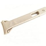
- Precision Wafer Handling Tool: Designed for safe and precise handling of silicon wafers, semiconductor chips, and flat substrates during inspection, processing, evaporation, and laboratory applications.
- High-Purity PEEK Material Construction: Made from high-performance PEEK (Polyether Ether Ketone) polymer, offering excellent mechanical strength, low contamination characteristics, and suitability for semiconductor and precision laboratory environments.
- High Temperature & Chemical Resistance: PEEK material provides excellent thermal stability and supports short-term exposure up to approximately 300°C while maintaining strength and dimensional stability. Resistant to many chemicals and solvents.
- Flat Tip Wide Jaw Design: Features a flat tip and wide gripping jaw structure to provide stable and gentle handling of delicate wafers and flat samples while reducing surface contact impact.
- Low Outgassing & Long-Term Durability: Designed with low outgassing, low moisture absorption, wear resistance, and excellent dimensional stability, making it suitable for cleanroom, semiconductor fabrication, research, and inspection applications.
ASML’s investor calendar scheduled its Q3 2026 results for October 14, 2026. Until that release, Q2 is the latest reported quarter covered here. ASML investor calendar
Quick Recap
Best Value
- for ultimate for surface Protection: Crafted from for premium PEEK material, these flat-tip tweezers for ensure scratch-free handling of sensitive wafers and semiconductors by point-loading damage during critical assembly tasks.
- Advanced for esd Safety: Designed with inherent anti-static properties to safely dissipate electrostatic charges, protecting delicate microelectronics and fiber optic components from discharge damage in cleanroom environments.
- Extreme Durability & Resistance: Withstands temperatures from -200°C to +260°C and resists harsh acids and alkalis used in etching, making these non-magnetic tools for ideal for diverse industrial and lab applications.
- for versatile Precision Toolset: Perfect for electronics repair, jewelry making, model building, and device assembly; the ergonomic design offers superior grip for long-term use in detailed soldering or inspection work.
- Reliable Quality Assurance: We stand behind our precision instruments with dedicated customer support; contact us immediately for any issues regarding product performance or satisfaction for a hassle-free resolution.
Product prices and availability are accurate as of the date/time indicated and are subject to change. Any price and availability information displayed on Amazon at the time of purchase will apply.




