The Tool Desk
Outbyte Driver Updater FREEScan for outdated or missing drivers - takes under a minuteDriver Scan →Outbyte PC Repair FREERepair Windows errors before they cause bigger problemsFix Now →Short answer: In TSMC’s published comparisons, newer process generations promise better performance, lower power use, and greater density—but the figures apply to particular process variants and comparison conditions, not every chip carrying a “2nm,” “3nm,” or “5nm” label. The cost estimates point in the other direction: advanced-node chip design and wafer production can be substantially more expensive.
For consumers, a smaller node does not automatically mean a faster, cheaper, or more efficient device. The chip’s design, workload, power limits, manufacturing yield, and product pricing all matter.
What 2nm, 3nm and 5nm mean
These labels identify generations of semiconductor manufacturing processes, often called nodes. They are useful shorthand for a foundry’s technology roadmap, but they are not literal measurements of a transistor’s size and do not provide a universal ruler for comparing different companies’ processes.
The exact process variant matters, too. The comparisons below use TSMC’s N5, N3E and N2P figures. They should not be generalized to every manufacturer’s 5nm, 3nm or 2nm process.
How TSMC’s published performance and power figures compare
TSMC reports process-level estimates for two transitions: N5 to N3E, and N3E to N2P. Each comparison uses its own baseline and operating condition.
| Comparison | Performance | Power | Density |
|---|---|---|---|
| TSMC N3E versus N5 | About 20% greater speed | More than 30% lower power | About 1.6 times the logic density |
| TSMC N2P versus N3E | About 18% higher performance at the same power | About 36% lower power at the same speed | About 20% greater transistor density |
These are TSMC’s estimates, not independent head-to-head measurements of finished retail chips. The N2P power and performance claims describe different operating points: higher performance at equal power is not the same comparison as lower power at equal speed. TSMC also describes density differently in the two comparisons—“logic density” for N3E versus N5 and “transistor density” for N2P versus N3E—so the figures should not be treated as one uniform scale. TSMC’s process comparison
Rank #2

- IC Type: Semiconductor
- Each wafer fragment contains visible integrated circuit patterns for demonstration and display purposes only.
- Made from single-crystal silicon wafer material for authentic semiconductor teaching and research.
- Ideal for electronics courses, microfabrication demonstrations, and STEM student projects.
- Also suitable for art installations, photography props, and chip design exhibitions.
What the figures mean for a finished chip
A process-level improvement is an option available to chip designers, not a guaranteed improvement in every product. A chip’s actual speed and power use depend on its architecture, design choices, operating voltage, workload, cooling and power limits. A manufacturer may use a newer process to increase performance, reduce power, fit more logic into a given area—or balance those goals.
- For performance: a newer process can support faster operation, but the finished chip’s design and product settings determine whether that potential is realized.
- For battery life: lower process-level power at a specified speed can help, but total device power also depends on other components and how the device is used.
- For size and capability: greater density can let designers fit more transistors into an area; it does not by itself establish how much faster a device will feel.
Why 2nm chips can cost more to develop and manufacture
Moving to a more advanced process can raise costs at several stages. A 2025 CSIS report reproduces projected system-on-chip advanced design costs of $449 million at 5nm, $581 million at 3nm and $725 million at 2nm. These are estimates for designing a chip for a process—not a foundry quote, the manufacturing cost of one chip, or a device’s retail price. The report also estimates 2nm wafer production cost at $30,000, about 50% above 3nm; that is an estimate, not a disclosed contractual wafer price. CSIS’s 2025 report
Outdated Drivers Are Slowing You Down
One free scan finds every outdated or missing driver and matches the right update for your exact hardware.Free scan · exact hardware matchPC Slower Than It Used to Be?
A free scan shows the junk files, broken settings and background clutter dragging Windows down - then fixes them in one click.Free scan · Windows 10 & 11Rank #3
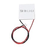
- Semiconductor thermoelectric chip TGM-199-1.4-0.8
| Cost measure | What it covers | What it does not tell you |
|---|---|---|
| Design cost | Estimated engineering and implementation expense to create a chip for a process node. CSIS reports projections of $449 million at 5nm, $581 million at 3nm and $725 million at 2nm. | The price of an individual chip or finished device. |
| Wafer production cost | The estimated cost associated with manufacturing a wafer. CSIS estimates $30,000 for a 2nm wafer, about 50% above 3nm. | The cost of each usable die or a foundry’s quoted price to a particular customer. |
| Cost per good die | Depends in part on wafer cost, die size, how efficiently dies fit on the wafer and manufacturing yield. | Cannot be calculated from wafer cost alone. |
| Retail chip or device price | Also reflects factors such as packaging, memory, product design, supply and the seller’s pricing. | Is not established by process-node design or wafer estimates alone. |
SEMI’s June 2025 presentation likewise describes rising wafer and design costs as process complexity grows, and says the performance, power and area benefits need to make sense at the system level. It does not provide a sufficiently legible node-by-node wafer-price series to support additional precise figures. SEMI’s market-intelligence materials
Process maturity matters as well as node generation
TSMC says its N2 technology uses its first generation of nanosheet transistors and began volume production in the fourth quarter of 2025. In its 2025 annual report, TSMC said N3 had entered its fourth year of volume production and N5 its fifth. That gives N5 and N3 longer production histories than N2 in the information cited here, but it does not establish comparable yield rates or prove that one process will be more available for every customer or product. TSMC N2 technology · TSMC 2025 Annual Report
Rank #4

- AUTHENTIC BARE DIE APPEARANCE-- Displays the exposed structure of a semiconductor die before final packaging, providing a direct view of chip layout and microelectronic design features.
- INTEGRATED CIRCUIT REFERENCE SAMPLE --Features visible IC circuitry and semiconductor architecture, making it a useful reference piece for understanding chip manufacturing concepts.
- IDEAL FOR TECHNICAL EDUCATION --Suitable for engineering courses, electronics training, semiconductor learning and STEM activities where physical examples support technical instruction.
- DISPLAY AND PRESENTATION USE --Can be incorporated into technology exhibitions, laboratory displays, classroom demonstrations and microelectronics presentations.
- COLLECTIBLE TECHNOLOGY ARTIFACT-- Combines semiconductor engineering with visual appeal, making it suitable for collectors, electronics enthusiasts and technology-themed displays.
Why a 2nm label does not establish a cross-company winner
Foundries use their own process names and technology roadmaps. Samsung describes SF2 as a second-generation MBCFET technology and its 3nm process as using a gate-all-around (GAA) architecture. Intel describes its 18A process as using RibbonFET transistors and PowerVia backside power delivery. These features provide context about the companies’ technologies, but the cited official materials do not supply a common set of performance, power, density and cost benchmarks for a direct comparison with TSMC. A node name alone therefore cannot establish which company’s process is objectively best. Samsung Foundry process technology · Intel process technology
Independent reader supportYour contribution helps us test, update, and keep practical guides available for everyone.How to judge a chip or device purchase
If you are comparing products, use product-specific evidence rather than the node label as a shortcut. Check independent reviews and specifications for the workloads, battery life, performance and price that matter to you. A process-generation claim can help explain how a chip was made; it cannot substitute for testing the finished product or comparing its total cost.
Quick Recap
Best Value

- AUTHENTIC BARE DIE APPEARANCE-- Displays the exposed structure of a semiconductor die before final packaging, providing a direct view of chip layout and microelectronic design features.
- INTEGRATED CIRCUIT REFERENCE SAMPLE --Features visible IC circuitry and semiconductor architecture, making it a useful reference piece for understanding chip manufacturing concepts.
- IDEAL FOR TECHNICAL EDUCATION --Suitable for engineering courses, electronics training, semiconductor learning and STEM activities where physical examples support technical instruction.
- DISPLAY AND PRESENTATION USE --Can be incorporated into technology exhibitions, laboratory displays, classroom demonstrations and microelectronics presentations.
- COLLECTIBLE TECHNOLOGY ARTIFACT-- Combines semiconductor engineering with visual appeal, making it suitable for collectors, electronics enthusiasts and technology-themed displays.
Product prices and availability are accurate as of the date/time indicated and are subject to change. Any price and availability information displayed on Amazon at the time of purchase will apply.




