Do these 3 things before closing this tab:
1Fix the driver behind crashes, sound loss and screen glitches2Repair Windows errors before they cause bigger problems3Scan for outdated or missing drivers - takes under a minuteSynopsys supplies electronic design automation (EDA) software and semiconductor IP; TSMC supplies manufacturing processes and advanced packaging. Their collaboration is a continuing effort to enable Synopsys tools and IP for TSMC technologies—not a single joint product or a guarantee that a customer design will meet its performance, cost, or production targets.
The partnership began receiving broad attention in 2024 and has since added announcements on TSMC’s N2P and A16 processes, multi-die packaging, silicon IP, and A14-related design flows. The latest identified public update, dated April 22, 2026, reports several specific milestones, but does not establish that every mentioned technology is generally available or in volume production.
What the collaboration covers
The work connects four parts of advanced-chip development: foundry-specific design flows, multi-die and package design, AI-assisted EDA, and reusable silicon IP. Synopsys develops the tools and IP; TSMC provides the process technologies, design rules, and packaging platforms those tools and blocks must support. The companies describe flows as certified or enabled for specified technologies. That is useful evidence of technical coordination, not a performance warranty for an individual customer design.
EDA flows for TSMC processes
Synopsys tools cover digital implementation, analog design and migration, physical verification, and power, performance, and area (PPA) optimization. A certified flow is validated against a stated set of foundry rules, process-design-kit (PDK) versions, tools, or reference conditions. Certification scope matters: a different process option, tool release, PDK revision, or design methodology may require further qualification. The customer remains responsible for design-specific verification and signoff.
Free tools Windows power users keep installed
One-click scans. No signup required.
#1 Best Overall

- ESP32-S3-ePaper-1.54 development board onboard 1.54inch e-paper display, 200 × 200 resolution, features high contrast and wide viewing angle. Onboard audio codec chip, supports voice capture and playback, enabling AI voice interaction applications
- ESP32-S3 1.54inch e-Paper AIoT development board adopts high-performance 32-bit LX7 dual-core processor, up to 240MHz main frequency. Supports 2.4GHz Wi-Fi (802.11 b/g/n) and Bluetooth 5 (LE), with onboard antenna
- Onboard PCF85063 RTC chip and SHTC3 temperature & humidity sensor for accurate RTC management and environmental monitoring
- Built-in 512KB Static RAM, 384KB ROM, with integrated 8MB Flash and 8MB PSRAM
- Onboard TF card slot for external storage of images or files. Onboard programmable PWR and BOOT side buttons for customized function development. Reserved 2 × 6 2.54mm pitch pin header for convenient external expansion
Multi-die and 3D design
Synopsys positions 3DIC Compiler as an exploration-to-signoff environment for multi-die systems. Its described functions include die and package planning, UCIe and HBM routing, TSV and bump planning, multi-die verification, and support for the 3Dblox framework. TSMC contributes packaging and integration technologies including CoWoS and SoIC. A package is part of the architecture in these systems: geometry, power delivery, heat flow, signal integrity, assembly, and test constraints affect the design alongside the individual dies.
In a 2.5D arrangement, multiple dies sit side by side and communicate through an interposer or advanced substrate. In 3D stacking, dies are placed vertically and connected using vertical interconnect technologies. “Multi-die” is the broader term for systems built from chiplets, stacked dies, interposers, bridges, or other heterogeneous combinations. These approaches can enable more compute and memory bandwidth, but add integration and manufacturing challenges.
AI-assisted design tools
Synopsys.ai and related capabilities apply optimization and automation to design tasks such as exploring implementation choices and improving QoR—quality of results across metrics including performance, power, area, and design time. They are tools for engineers, not evidence that chip design has become fully autonomous. Synopsys’ April 2026 announcement specifically reports agentic run assistance in Fusion Compiler for TSMC A14 using NanoFlex Pro architecture; that milestone does not establish routine, fully autonomous commercial design.
Reusable silicon IP
Synopsys offers interface, foundation, memory, networking, automotive, and other IP intended to spare customers from building every block from scratch. Announcements refer to technologies including UCIe, HBM, PCIe, Ethernet, MIPI, USB, DDR5 MR-DIMM, LPDDR5X and LPDDR6, M-PHY, and photonics-related IP. “Silicon-proven” means the vendor reports prior silicon validation or implementation evidence. It does not remove the need to integrate, verify, and validate the block in the customer’s design and system.
What’s actually slowing this PC down?
Pick the symptom - the matching free tool is one click away.
Rank #2

- This is is 1.54inch e-Paper AIoT development board. Onboard 1.54inch e-paper display, 200 x 200 resolution, features ultra-low power consumption and ambient light readability, suitable for portable devices and long-battery-life scenarios. Supports 2.4GHz Wi-Fi (802.11 b/g/n) and Bluetooth 5 (LE), with onboard antenna.
- Integrated with an RTC chip, SHTC3 temperature and humidity sensor, TF card slot, low-power audio codec chip circuit, and Lithium battery recharge management circuit. Reserved interfaces including USB, UART, I2C, and GPIO for easy functionality expansion and sensor connectivity, providing a flexible and reliable development platform for IoT terminals, electronic tags, portable displays, and other applications.
- Supports AI Speech Interaction: Allows access to online large model platforms such as ChatGPT, DeepSeek, Doubao, etc. Onboard audio codec chip, supports voice capture and playback, enabling AI voice interaction applications.
- Built-in 512KB Static RAM, 384KB ROM, with integrated 8MB Flash and 8MB PS RAM. Onboard PCF85063 RTC chip and SHTC3 temperature & humidity sensor for accurate RTC management and environmental monitoring.
- Onboard TF card slot for external storage of images or files. Onboard programmable PWR and BOOT side buttons for customized function development. Reserved 2 × 6 2.54mm pitch pin header for convenient external expansion.
Why AI systems are pushing toward multi-die design
AI systems need growing amounts of compute and memory bandwidth. Designers can respond with larger dies, multiple compute dies, high-bandwidth memory (HBM), or combinations of these. A single die is constrained by reticle limits, while advanced packaging can bring compute and memory closer together. That can improve bandwidth and energy efficiency, but increases demands on cooling, power delivery, assembly, test, and verification.
- Memory bandwidth: HBM and wide die-to-die links require careful placement and high-speed interconnect design.
- Power and heat: Dense compute creates power-delivery and thermal challenges that span die and package.
- Manufacturing constraints: Leading-edge processes, large interposers, and advanced assembly introduce rules and yield considerations beyond conventional chip design.
- System-level optimization: The right trade-off depends on the package, workload, memory configuration, and production economics—not just the transistor process.
The “trillion-transistor” phrase in the 2024 announcement describes the direction of aggregate system complexity across future multi-die designs. It should not be read as a claim that one monolithic TSMC chip already contains one trillion transistors.
Which TSMC technologies are involved
N2 and N2P
N2 is TSMC’s 2nm-class process family; N2P is an enhanced process in the same general generation. Synopsys announcements describe digital and analog flows, Synopsys.ai enablement, and IP work for N2 and N2P. A node name alone does not determine a finished chip’s speed, power, density, yield, or cost. Designers need to confirm the specific process option, PDK maturity, IP readiness, and manufacturing schedule for their program.
A16 and backside power delivery
TSMC A16 is associated in the announcements with Super Power Rail (SPR), a backside power-delivery approach. Moving or reorganizing power distribution relative to conventional frontside routing can free routing resources and support power delivery, but it also brings new design, verification, thermal, and manufacturing considerations. Synopsys says its certified capabilities address power distribution, performance, thermal robustness, and pattern-based pin access; the public announcements do not supply a comparable customer benchmark establishing a universal PPA gain.
Quick wins for a faster PC:
Scan for outdated or missing drivers - takes under a minuteDriver Scan →Clear out junk files and repair common Windows errorsFree Scan →Fix the driver behind crashes, sound loss and screen glitchesFind Drivers →Rank #3
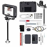
- 【Flagship performance, extremely fast response】Equipped with a 1.6GHz main frequency chip, the KPU computing power is 13.7 times that of the K210 visual module, and the CPU computing power is 8.5 times that of the K210. It supports real-time operation of complex AI models and can easily cope with high-load tasks such as image recognition and voice processing.
- 【Flexible expansion development】A new 12Pin GPIO interface is added, which is compatible with a variety of sensors and modules; pre-installed GUI program, a large program based on the RTSmart system, contains 30+ functional gameplay, integrates most of the core functions, and each function comes with instructions, so you can experience the fun of AI without programming basics.
- 【Multi-controller compatibility】Equipped with a serial communication interface, it can be seamlessly connected to various controllers, and supports connection to PC computers, MSPM0, STM32, ESP32, PICO, Raspberry Pi, UNO, Microbit, Jetson, RDK and other mainstream controller development. You can easily output the visual recognition results to an external controller through the serial port without delving into complex visual algorithms, making it easy to create innovative AI projects.
- 【Multi-function AI visual camera】The K230 visual module is equipped with a 2.4-inch LCD capacitive touch screen with clear display and a 2MP camera for quick debugging and control. The module integrates a serial port, which can easily connect various sensors to expand functions. , with color recognition, road sign recognition, visual line patrol, face recognition, label recognition, QR code and barcode recognition, feature detection, digital recognition and other functions.
- 【Developers from entry to mastery】Provides original model training tutorials+self-developed upper computer toolkits, compatible with ESP32 ecology, suitable for education, maker and industrial visual project development. Yahboom provides technical Q&A + lifetime firmware updates to help your AI project from prototype to landing without worry!
A14 and design-flow maturity
The September 2025 announcement described A14 flow development and anticipated a first PDK release in the latter part of 2025. The April 2026 announcement later cited Fusion Compiler agentic run assistance for A14 with NanoFlex Pro. Flow development, PDK availability, IP readiness, customer design starts, tape-outs, and volume manufacturing are separate milestones. The cited updates do not by themselves establish broad A14 availability or production status.
3DFabric, SoIC, CoWoS, and 3Dblox
TSMC’s 3DFabric family covers advanced packaging and 3D integration. CoWoS is a chip-on-wafer-on-substrate packaging family; SoIC is TSMC’s 3D stacking technology. 3Dblox is a framework for describing and integrating 3D IC designs. Synopsys’ 2026 update says 3DIC Compiler supports CoWoS packages using interposers described as 5.5 times reticle size. That is a reported tool-support milestone, not proof that every customer can immediately manufacture an economical package at that scale. Feasibility depends on product design, assembly, substrate capacity, thermal requirements, and yield.
How the partnership has developed
| Date | What the companies reported |
|---|---|
| April 24, 2024 | Synopsys described digital and analog flows for TSMC N3/N3P and N2, plus physical-verification, photonics, and IP collaboration. Synopsys announcement |
| September 25, 2024 | The companies announced broader AI-driven EDA, advanced-process, 3DFabric, multi-die, photonics, UCIe, HBM4, and 3DIO-related work. The release framed “trillion-transistor” design as a future multi-die challenge. Synopsys announcement |
| April 23, 2025 | Synopsys announced certified flows for TSMC A16 and N2P, work on 3Dblox and CoWoS, and IP development involving HBM4, 1.6T Ethernet, UCIe, PCIe 7.0, and UALink. Synopsys announcement |
| September 24, 2025 | Synopsys reported multiple customer tape-outs using 3DIC Compiler with TSMC SoIC and CoWoS, alongside certified N2P and A16 flows. The public release did not identify those customers. Synopsys announcement |
| April 22, 2026 | Synopsys reported M-PHY v6.0 silicon bring-up on N2P, a 64G UCIe IP tape-out, 224G IP development, A14 agentic run assistance, and 3DIC Compiler support for 5.5× reticle-size CoWoS interposers. Synopsys announcement |
What has been demonstrated—and what remains unproven publicly
The announcements describe different types of progress that should not be conflated. A certified flow indicates validation within a stated scope; a tape-out means a design was sent for fabrication; silicon bring-up reports testing or initial operation of silicon. None alone demonstrates successful volume production or commercial product economics.
- Customer tape-outs: Synopsys says its 3DIC Compiler and related IP supported multiple customer tape-outs involving TSMC SoIC and CoWoS; the cited release does not name the customers.
- Silicon and IP milestones: Synopsys reports M-PHY v6.0 silicon bring-up on N2P, a 64G UCIe IP tape-out, and development work on 224G IP.
- Earlier flow claims: The 2024 announcement described production-ready AI-driven flows on N2 and joint multi-physics work involving TSMC, Synopsys, and Ansys for CoWoS interposer designs.
- Not disclosed in the cited releases: comparable PPA measurements, yield, total design cost, production volumes, customer identities for the reported tape-outs, or a complete orderability schedule for every IP block.
These are company-reported milestones, not independent evidence of performance gains across customer products. In 2024, Synopsys also announced 3DSO.ai for AI-driven 3D design-space optimization; its existence is a capability announcement, not a disclosed benchmark of customer outcomes. Synopsys announcement
Rank #4

- High-Performance AI Voice Interaction Development Board: Features a dual-core RISC-V processor (up to 160MHz), onboard dual microphone array, speakers, and an ES8311 audio codec chip, supporting noise reduction and echo cancellation. It can easily connect to large online models like DeepSeek for intelligent voice dialogue.
- Integrating Advanced Wireless Connectivity: ESP32-C6 supports Wi-Fi 6, Bluetooth 5.0, and Zigbee 3.0/Thread protocols, boasting excellent RF performance and multi-protocol compatibility, making it suitable for wireless communication development in IoT and wearable devices.
- Equipped with a 1.83-inch capacitive touchscreen LCD: (240×284 resolution, 65K colors), it offers high responsiveness and light transmittance. Combined with an onboard six-axis sensor (accelerometer + gyroscope) and RTC chip, it supports motion monitoring, step counting, and low-power real-time clock applications.
- Low Power Design: built-in Batt. recharge chip, a Type-C interface, and supports flexible clock and power control, enabling low-power operation in various scenarios, making it convenient for carrying around and long-term use.
- Rich Interfaces: It offers a wealth of expansion interfaces and customization features, including GPIO, I2C, and UART pads, two programmable side buttons, support for external sensors and debugging, and facilitates rapid prototyping and functional verification.
What chip companies should evaluate
EDA flow fit
- Confirm coverage for the exact node, process option, PDK version, and tool release—not just the node family.
- Ask which tools and checks are included in certification, and whether digital, analog, physical-verification, and package-level work are covered.
- For AI-assisted optimization, assess reproducibility, auditability, engineer override, regression testing, and protection of proprietary design data.
- Check interoperability with package, thermal, mechanical, and manufacturing workflows, as well as compute and licensing requirements.
- Request evidence behind claimed productivity or QoR improvements, including the design, baseline, constraints, and measurement method.
IP readiness
- Verify interface standard revision, compliance status, process qualification, speed and voltage ranges, and PVT-corner coverage.
- Check whether the block is available, certified, silicon-proven, taped out, or still in development; those terms describe different stages.
- Review verification collateral, drivers, security features, automotive safety evidence where relevant, package assumptions, licensing terms, and reuse rights.
- Validate the IP in the intended package and system, including interoperability with HBM, UCIe, PCIe, Ethernet, MIPI, or M-PHY as applicable.
Packaging and product economics
- Compare a monolithic SoC with chiplets, 2.5D interposer designs, and 3D stacking for the product’s workload and schedule.
- Model total package cost, including interposer or substrate, assembly, test, cooling, and known-good-die strategy—not only wafer cost.
- Check HBM, substrate, interposer, and assembly capacity, along with repair, binning, lifecycle, and second-source considerations.
- Account for die-to-die latency, thermal hotspots, test complexity, security boundaries, and software partitioning.
Commercial implications
This is an enterprise semiconductor-tooling and design-services story, not a self-serve software purchase. Synopsys, TSMC, and other EDA vendors do not generally publish list prices for the advanced-node licenses, IP, and foundry access relevant here. Costs and eligibility depend on the project, tool scope, IP licensing, compute, support, process access, and commercial terms; no fixed price can be inferred from the announcements.
Teams can review Synopsys’ TSMC partnership overview, its EDA portfolio, DesignWare IP, 3DIC Compiler, and Synopsys.ai. TSMC’s Open Innovation Platform describes its foundry ecosystem. Cadence, Siemens EDA, and Ansys are also relevant suppliers for particular implementation, verification, package, or multiphysics requirements; compare actual certified coverage, workflow fit, and migration cost rather than assuming one vendor is categorically better. See Cadence, Siemens EDA, and Ansys.
For a project without internal advanced-node or 3D-IC expertise, a design-services firm or turnkey provider may be worth evaluating, but selection should be based on verified foundry access, tape-out experience, package engineering, verification ownership, NRE terms, and long-term support. The collaboration is most relevant to organizations with a qualified TSMC program and a real need for leading-edge or multi-die design; a mature-node project may not justify the technical and commercial overhead.
Quick Recap
Product prices and availability are accurate as of the date/time indicated and are subject to change. Any price and availability information displayed on Amazon at the time of purchase will apply.




