Short answer: The United States and India are building a broader framework for semiconductor and technology cooperation, not announcing one jointly owned chip factory. Their March 10, 2023 memorandum of understanding (MOU) created a mechanism for supply-chain resilience, diversification, commercial links, research and workforce development. Since then, the relationship has expanded through the TRUST technology framework and India’s February 2026 entry into the U.S.-led Pax Silica initiative.
What the 2023 agreement actually was
The semiconductor-specific agreement signed during the U.S.–India Commercial Dialogue in New Delhi on March 10, 2023, was a memorandum of understanding establishing a Semiconductor Supply Chain and Innovation Partnership. The U.S. Department of Commerce described it as a collaborative mechanism rather than a procurement contract or construction agreement. Its objectives include supply-chain resilience and diversification, coordination around the U.S. CHIPS and Science Act and India’s Semiconductor Mission, commercial opportunities, research and development, and semiconductor talent. (U.S. Department of Commerce; India Press Information Bureau)
That distinction matters. The MOU does not publicly specify a jointly owned fab, a total investment amount, a production quota, or a guaranteed source of chips. It is a framework for governments, companies, universities and research institutions to identify projects and coordinate policy.
How the partnership has expanded
| Date | Development | What it means |
|---|---|---|
| March 10, 2023 | Semiconductor Supply Chain and Innovation Partnership MOU | Creates a bilateral mechanism focused on resilience, diversification, trade, research and skills. |
| 2023–2024 | Commercial Dialogue and related technology cooperation | Officials continued discussions on semiconductor and innovation opportunities. |
| 2024 | GlobalFoundries Kolkata Power Center cited in a bilateral fact sheet | An example of research and ecosystem cooperation, not evidence of a leading-edge production fab. (Fact sheet) |
| February 13, 2025 | TRUST (“Transforming the Relationship Utilizing Strategic Technology”) | Places semiconductors within a wider U.S.–India technology agenda covering AI, quantum, biotechnology, energy, defense and space. (Joint statement; TRUST overview) |
| February 6, 2026 | Expanded economic-security cooperation | Joint language covers supply-chain resilience, investment reviews, export controls and technology trade. (White House statement) |
| February 20, 2026 | India joins Pax Silica | Gives the relationship a multilateral focus on secure semiconductor, critical-mineral and AI-infrastructure supply chains. (India Ministry of External Affairs) |
Why Washington and New Delhi want cooperation
Semiconductors depend on a geographically distributed chain: architecture and design, electronic-design automation, materials, equipment, wafer fabrication, assembly, testing, packaging, logistics and customer qualification. Concentration at any one stage can expose automakers, communications firms, data centers, defense suppliers and other industries to disruption.
#1 Best Overall

- COMPATIBILITY: Development board supporting multiple wireless protocols including Bluetooth
- Thread, Matter, Zigbee, ANT, and NFC at 2.4GHz frequency
- PROCESSOR: Features the advanced nRF54L15 transceiver chip from Nordic Semiconductor for reliable wireless communications
- WIRELESS STANDARDS: Implements IEEE 802.15.4 protocol support for Matter, Thread, and Zigbee networking applications
- DEVELOPMENT PLATFORM: Comprehensive evaluation board designed for testing and prototyping wireless connectivity solutions
The U.S. CHIPS and Science Act is intended to expand American manufacturing, research and workforce capacity while building trusted international networks. India’s India Semiconductor Mission offers financial and infrastructure support for semiconductor and display manufacturing, packaging and related design capabilities. The 2023 MOU is intended to help the countries find complementary projects rather than duplicate every investment.
Official statements emphasize resilience, diversification, trusted vendors and economic security. Those goals are consistent with reducing exposure to China-dominated parts of the technology supply chain, but the documents do not describe the MOU as a completed anti-China alliance. The 2026 economic-security statement adds cooperation on investment screening and export controls, areas where geopolitical competition is an important context.
Rank #2

- Powerful ESP-32 Board: Unlock the world of Internet of Things (IoT) and advanced electronics with the heart of this kit: the ESP-32 board. It features a powerful dual-core processor, integrated Wi-Fi and Bluetooth 4.2, making it perfect for building connected, smart devices that communicate with your phone or the cloud. It's fully compatible with the Arduino IDE for easy programming.
- Super Starter Kit: This kit contains over 35 different modules and electronic components, including sensors, displays, motors, and input devices. From LEDs and buttons to an OLED screen, servo motor, and keypad, you have everything needed to explore a vast range of projects in one box.
- Step by Step Online Tutorial: Jump right in with our detailed, beginner-friendly tutorial. Access 30+ projects with complete code, clear circuit diagrams, and step-by-step instructions. Learn the fundamentals of electronics, coding, and how to utilize the ESP-32's unique capabilities without any prior experience.
- Hands-on Learning for All Skill Levels: Perfect for students, makers, engineers, and hobbyists. Start with basic circuits and coding, then progress to intermediate and advanced IoT applications. Build practical projects like weather stations, smart home controllers, remote-controlled devices, and interactive gadgets. The skills you learn are the foundation for real-world innovation.
- Quality & Great Support: Elegoo is committed to quality. We provide a clear, detailed tutorial guide, refined code, and a well-organized component kit. All modules are carefully selected for reliability and ease of use. Our dedicated technical support team and active online community are ready to help you succeed in your learning journey.
What the United States can contribute
- Advanced chip design, intellectual property and electronic-design-automation expertise.
- Semiconductor equipment, research institutions, capital and experienced manufacturing companies.
- CHIPS-related incentives and technology-security programs.
- University, laboratory and workforce partnerships.
- Large customer markets in advanced computing, vehicles, communications, defense and data centers.
The United States does not control every stage of global production. Much of its semiconductor ecosystem is international, and export controls and national-security rules can limit which technologies or suppliers are available for cooperation.
What India can contribute
- A large engineering, software and chip-design workforce.
- Experience in design services and chip-development support.
- Electronics-manufacturing ambitions and a growing domestic market.
- Government incentives through the India Semiconductor Mission.
- Potential capacity in assembly, testing, packaging, specialty manufacturing and design.
- A strategic position in discussions about critical minerals and technology supply chains.
India is still developing large-scale commercial wafer-fabrication capacity and a complete local supplier base. Its fastest opportunities may therefore be in design, packaging, testing and selected specialty or power-semiconductor segments rather than immediately matching the most advanced logic production in East Asia.
The Tool Desk
Outbyte PC Repair FREEClear out junk files and repair common Windows errorsFree Scan →Outbyte Driver Updater FREEScan for outdated or missing drivers - takes under a minuteDriver Scan →Rank #3

- DEVELOPMENT KIT: Nordic Semiconductor NRF5340-AUDIO-DK designed for audio application development with nRF5340 dual-core Bluetooth LE SOC
- VERSATILE CONNECTIVITY: Features multiple interface options including I2S, SPI, UART, and USB for comprehensive development capabilities
- POWER SPECIFICATIONS: Operates with flexible power supply range of 1.7V to 5V, suitable for various development scenarios
- TEMPERATURE RANGE: Capable of operating in environments up to +105°C, ensuring reliable performance across diverse conditions
- AI COMPATIBILITY: Supports Edge Impulse platform integration, enabling advanced machine learning and AI development capabilities
What “strengthening the supply chain” means in practice
| Layer | Possible cooperation |
|---|---|
| Design | Chip architecture, verification, intellectual property and design software. |
| Manufacturing | Wafer fabrication, including specialty processes as well as advanced logic. |
| Packaging and testing | Assembly, testing, marking and advanced packaging that connect chips to usable products. |
| Materials | Wafers, gases, chemicals, photoresists and other process inputs. |
| Equipment | Lithography, deposition, etching, metrology and packaging machinery. |
| Talent and research | Engineers, technicians, operators, researchers, managers and joint R&D programs. |
| Trade and investment | Incentives, export controls, investment reviews, supplier qualification and market access. |
| Logistics and security | Trusted vendors, data protection, secure transport and continuity planning. |
This wider definition explains why a research center, packaging plant or design program can be strategically useful without being equivalent to a leading-edge fab.
The GlobalFoundries Kolkata Power Center
A 2024 India–U.S. fact sheet highlighted GlobalFoundries’ creation of the GF Kolkata Power Center. The project was described as strengthening research and development links involving chip manufacturing and supporting applications such as connected vehicles, Internet of Things devices, artificial intelligence and data centers. The public description does not establish that it is a complete semiconductor ecosystem or a leading-edge commercial production plant. (India–U.S. fact sheet)
Rank #4

- VERSATILE CONNECTIVITY: Supports both Bluetooth
- And IEEE 802.15.4 protocols (Thread, Zigbee) for comprehensive wireless development capabilities
- DEVELOPMENT PLATFORM: Complete development kit for nRF5340 System-on-Chip applications with integrated debugging and programming capabilities
- DUAL-CORE ARCHITECTURE: Features both application and network processing cores for enhanced wireless development flexibility
- WIRELESS PROTOCOLS: Designed for 2.4GHz wireless applications including Bluetooth Low Energy and 802.15.4-based protocols
What TRUST and Pax Silica add
TRUST broadens semiconductor cooperation into a government, academic and private-sector technology framework. It also introduces a trusted-vendor approach for sensitive technologies and links chips with AI, quantum systems, biotechnology, energy, defense and space.
Pax Silica is broader still. Its stated focus is secure and resilient supply chains for semiconductors, critical minerals and the infrastructure supporting the AI economy. India’s accession places it in a wider network of U.S. partners and gives the bilateral relationship a multilateral economic-security dimension. Joining a declaration or initiative is not the same as announcing a fab, financing package, production quota or legally binding supply guarantee. (White House science and technology highlights)
Free tools Windows power users keep installed
One-click scans. No signup required.
Best Value
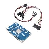
- POWER MONITORING: Professional-grade current monitoring and power management evaluation board for precise power consumption analysis
- COMPATIBILITY: Designed specifically for Nordic Semiconductor development and testing applications
- MEASUREMENT CAPABILITIES: Enables real-time current measurement and power profiling for embedded system development
- DATA ANALYSIS: Features comprehensive power consumption data collection and visualization capabilities
- DEVELOPMENT TOOL: Essential evaluation board for optimizing power efficiency in embedded system projects and prototypes
What has not been announced
- No public bilateral commitment to build one named U.S.–India semiconductor fab.
- No publicly stated total investment figure for the 2023 MOU.
- No guaranteed percentage of semiconductor supply sourced from India.
- No evidence that India can immediately replace Taiwan, South Korea, China, Japan or the Netherlands across every stage.
- No automatic exemption from export controls, investment screening, procurement rules or national-security restrictions.
Government intent also does not guarantee that a private project will secure financing, reach target yields, pass customer qualification or operate at commercial scale.
Trade-offs and practical constraints
- Resilience versus cost: geographically duplicated capacity can cost more than concentrated production.
- Security versus openness: trusted-vendor rules and export controls can protect sensitive technology while narrowing participation.
- Speed versus capability: packaging, design and specialty capacity can generally expand faster than leading-edge wafer fabrication.
- Incentives versus efficiency: subsidies may attract investment but can also create overlapping or politically driven projects.
- Talent bottlenecks: experienced process engineers, technicians and plant operators remain difficult to develop quickly.
- Policy uncertainty: tariffs, export controls, subsidies and investment rules can change the economics of a project.
How to judge whether the partnership is delivering
- Look for named companies, facilities, funding amounts and construction or production schedules—not just declarations.
- Identify the supply-chain layer involved: design, fabrication, packaging, materials, equipment, research or workforce.
- Check whether commitments are grants, contracts, preliminary terms or completed private investment.
- Track joint R&D projects, university programs, supplier qualifications and cross-border trade.
- Measure commercial production, yields, customer qualification and reduced concentration in specific categories.
The first visible effects are most likely to appear in industrial policy, investment decisions, design work, packaging, specialty chips, workforce programs and supplier qualification. A complete substitute for established East Asian manufacturing networks would require far larger capital commitments, supplier depth and years of qualification.
The Bottom Line
The U.S.–India semiconductor partnership is strategically real and expanding, but it remains a network of frameworks and projects rather than a single manufacturing deal. Its significance will be demonstrated by funded facilities, operating capacity, joint research, trained workers and measurable diversification—not by the MOU or Pax Silica membership alone.
Quick Recap
Product prices and availability are accurate as of the date/time indicated and are subject to change. Any price and availability information displayed on Amazon at the time of purchase will apply.
Recommended Free Tools




