Recommended Free Tools
Samsung has reportedly secured advanced High-NA EUV lithography equipment from ASML, but that is not the same as buying a machine that automatically builds a 2nm chip—or proves the Exynos 2600’s performance claims. Samsung confirms the Exynos 2600 is based on its 2nm gate-all-around (GAA) process; it has not publicly tied the processor’s claimed gains to High-NA EUV. The equipment is strategically important for Samsung’s manufacturing roadmap, while its direct effect on this chip remains unestablished.
What Samsung reportedly acquired
The reported purchase concerns ASML High-NA EUV lithography scanners. Lithography equipment projects circuit patterns onto silicon wafers; it is one part of a much larger chipmaking process, not a complete “chip-building tool.”

In October 2025, TrendForce reported that Samsung planned to receive two ASML TWINSCAN EXE:5200B systems for production-oriented use by the first half of 2026. The report put the pair’s estimated cost at 1.1 trillion won, or about $773 million. Those details—including the model, count, timing, and price—are industry-reported, not specifications Samsung confirmed in its public report. Korea JoongAng Daily had also reported earlier High-NA equipment acquisition by Samsung in March 2025, so “finally acquires” overstates how new the development is. TrendForce’s account of the reported order and Korea JoongAng Daily’s coverage of High-NA adoption provide the industry-reporting context.
ASML’s January 28, 2026 presentation confirmed that an EXE:5200B was operating at a customer site. ASML said it had shipped eight High-NA systems in total, with six operating, but did not identify Samsung as the customer. It targeted high-volume-manufacturing readiness by the end of 2026 and customer insertion during 2027–2028. ASML’s presentation establishes the equipment’s status and timeline, not Samsung’s specific installation.
Free tools Windows power users keep installed
One-click scans. No signup required.
What High-NA EUV does—and what “2nm” means
High-NA EUV is a newer generation of extreme-ultraviolet lithography. Its numerical aperture is about 0.55, compared with roughly 0.33 for conventional EUV. Industry coverage describes that change as enabling about 1.7 times finer patterning. This is a measure of patterning capability, not a promise that a finished chip will be 1.7 times faster. TrendForce’s technical overview gives the reported comparison.
“2nm” is a process-generation label, not a literal measurement of every transistor feature, and High-NA is not synonymous with 2nm. Conventional EUV can be used to manufacture at advanced nodes; High-NA is an option for finer patterning and future scaling, not a universal prerequisite for a 2nm chip.
Using High-NA on critical layers could allow manufacturers to reduce some multi-patterning steps and create more process options. But a scanner alone does not determine chip performance or manufacturing success. Deposition, etching, materials, masks, metrology, transistor design, process integration, yield, packaging, and software all matter.
Rank #2

- IC Type: Semiconductor
- Each wafer fragment contains visible integrated circuit patterns for demonstration and display purposes only.
- Made from single-crystal silicon wafer material for authentic semiconductor teaching and research.
- Ideal for electronics courses, microfabrication demonstrations, and STEM student projects.
- Also suitable for art installations, photography props, and chip design exhibitions.
What Samsung confirms about Exynos 2600
Samsung’s 2026 interim report describes the Exynos 2600 as its first mobile application processor based on a 2nm GAA process. Samsung says its first-generation 2nm GAA process entered mass production in September 2025, with claimed improvements of 5% in performance, 8% in power consumption, and 5% in area versus its second-generation 3nm process. These are Samsung’s reported process comparisons, not independent measurements. Samsung’s interim report contains the company’s process and processor disclosures.
What’s actually slowing this PC down?
Pick the symptom - the matching free tool is one click away.
For the Exynos 2600 versus the Exynos 2500, Samsung claims:
- 39% higher CPU performance.
- 50% better GPU ray-tracing performance.
- 113% higher NPU AI performance.
Samsung also highlights a Heat Path Block intended to improve thermal performance, and says the processor supports camera sensors up to 230 megapixels and AI-based video enhancement. The performance figures are Samsung’s claims; they should not be treated as independently verified real-world results without third-party testing.
Rank #3
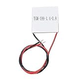
- Semiconductor thermoelectric chip TGM-199-1.4-0.8
Will High-NA EUV make the Exynos 2600 faster?
There is no public evidence establishing that the reported High-NA equipment produced the Exynos 2600’s claimed performance gains. Samsung attributes those gains to the processor and its 2nm GAA process, and discusses thermal design as part of the product story; its report does not say that High-NA EUV caused the improvements.
It is plausible that High-NA equipment could help Samsung learn, refine manufacturing processes, and prepare for later scaling. But given ASML’s stated high-volume readiness and customer-insertion timetable, it would be an inference—not a confirmed fact—to connect the newly reported production-oriented tools directly to the Exynos 2600. Samsung says its first-generation 2nm process was already in mass production from September 2025, before ASML’s stated broad High-NA insertion window.
Even if a process node offers efficiency gains, a phone may use that headroom for higher performance rather than longer battery life. Sustained speed and battery life also depend on the chip design, power limits, cooling, memory, packaging, firmware, and the phone itself. Samsung’s Heat Path Block addresses one part of that wider system; it does not establish how a finished device performs.
Rank #4

- AUTHENTIC BARE DIE APPEARANCE-- Displays the exposed structure of a semiconductor die before final packaging, providing a direct view of chip layout and microelectronic design features.
- INTEGRATED CIRCUIT REFERENCE SAMPLE --Features visible IC circuitry and semiconductor architecture, making it a useful reference piece for understanding chip manufacturing concepts.
- IDEAL FOR TECHNICAL EDUCATION --Suitable for engineering courses, electronics training, semiconductor learning and STEM activities where physical examples support technical instruction.
- DISPLAY AND PRESENTATION USE --Can be incorporated into technology exhibitions, laboratory displays, classroom demonstrations and microelectronics presentations.
- COLLECTIBLE TECHNOLOGY ARTIFACT-- Combines semiconductor engineering with visual appeal, making it suitable for collectors, electronics enthusiasts and technology-themed displays.
Why the investment matters to Samsung’s foundry strategy
High-NA access could give Samsung valuable experience with a technology expected to matter for future advanced logic and memory manufacturing. Its potential benefits depend on more than delivery:
- Installation and qualification: A delivered system must be installed, calibrated, and qualified with suitable masks, materials, and process steps before it can contribute to production.
- Layer selection: A manufacturer may use High-NA only on selected critical layers rather than throughout every layer of a chip.
- Yield and cost: The commercial test is whether the fab can produce enough usable chips at a viable cost, not just whether it can print finer features.
- Process and design readiness: Samsung’s GAA process, process-design kits, libraries, validated intellectual property, and design support all affect what customers can build and how reliably.
Samsung has said it expects to win additional customers for advanced logic chips, according to Reuters reporting carried by Investing.com. Securing equipment may support that ambition, but does not by itself demonstrate customer wins, competitive yields, or a cost advantage.
Independent reader supportYour contribution helps us test, update, and keep practical guides available for everyone.How Samsung’s position compares with competitors
High-NA adoption is part of a broader equipment and process race, but tool ownership alone does not rank foundries by manufacturing performance.
Quick wins for a faster PC:
Fix the driver behind crashes, sound loss and screen glitchesFind Drivers →Repair Windows errors before they cause bigger problemsFix Now →Scan for outdated or missing drivers - takes under a minuteDriver Scan →Best Value

- AUTHENTIC BARE DIE APPEARANCE-- Displays the exposed structure of a semiconductor die before final packaging, providing a direct view of chip layout and microelectronic design features.
- INTEGRATED CIRCUIT REFERENCE SAMPLE --Features visible IC circuitry and semiconductor architecture, making it a useful reference piece for understanding chip manufacturing concepts.
- IDEAL FOR TECHNICAL EDUCATION --Suitable for engineering courses, electronics training, semiconductor learning and STEM activities where physical examples support technical instruction.
- DISPLAY AND PRESENTATION USE --Can be incorporated into technology exhibitions, laboratory displays, classroom demonstrations and microelectronics presentations.
- COLLECTIBLE TECHNOLOGY ARTIFACT-- Combines semiconductor engineering with visual appeal, making it suitable for collectors, electronics enthusiasts and technology-themed displays.
| Company | What the cited reporting establishes | What it does not establish |
|---|---|---|
| Samsung | Industry reports described an earlier High-NA system and a plan for two EXE:5200B tools; ASML later confirmed an EXE:5200B at an unnamed customer site. | ASML did not identify Samsung as that customer in the cited presentation, and Samsung’s report does not give a confirmed machine count or link a specific tool to Exynos 2600. |
| Intel | Industry coverage associates Intel with earlier-generation High-NA equipment for future advanced-node development. | The cited material does not establish a directly comparable production yield, cost, or product-performance result. |
| TSMC | Industry reporting described High-NA use for research and development, with conventional EUV expected to continue through its 2nm node before later insertion. | Equipment access alone does not establish the comparative maturity or economics of a future node. |
| SK hynix | Korea JoongAng Daily reported installation of an EXE:5200B for production-oriented memory development and described SK hynix as the first memory manufacturer to adopt a High-NA tool for mass production. | That category-specific claim does not make SK hynix first among all semiconductor manufacturers or demonstrate commercial yields. |
The comparisons draw on Korea JoongAng Daily, TrendForce, and ASML’s January 2026 presentation. Their timelines and stated purposes differ, so declaring a winner based only on who acquired which scanner would be misleading.
What buyers and investors should watch next
For a consumer, the relevant test is how an Exynos-powered device performs in independent reviews: sustained speed, battery life, heat, and real-world camera and AI tasks matter more than the node label or scanner specifications. Availability can also vary by phone model and region; the equipment reports do not establish which Galaxy devices will use Exynos 2600.
For investors and industry watchers, the stronger signals are confirmed tool installations and production use, yield and cost progress, customer commitments, and whether Samsung can turn its 2nm process into reliable products at scale. Samsung’s public report confirms the Exynos 2600 and its 2nm process, while the specific High-NA purchase details remain based on industry reporting.
Quick Recap
Product prices and availability are accurate as of the date/time indicated and are subject to change. Any price and availability information displayed on Amazon at the time of purchase will apply.




