Intel Fab 9 began operations in the milestone sense on January 24, 2024—not in 2026. The Rio Rancho, New Mexico, facility is an advanced-packaging plant, not a conventional leading-edge logic-wafer fab. Its importance is that it gives Intel a U.S. high-volume site for assembling chiplets with Foveros 3D technology, alongside Fab 11X, as chiplet-based processors and AI systems become more important.
What Intel opened, and when
Intel celebrated Fab 9’s opening in Rio Rancho on January 24, 2024. The event marked the move from construction and equipment installation toward operational high-volume advanced-packaging manufacturing. It should not be read as proof that every tool was fully ramped or that the building reached full utilization that day.
The project was part of Intel’s originally announced $3.5 billion New Mexico investment to expand advanced semiconductor packaging, including Foveros. Later Intel materials describe broader New Mexico investment of more than $4 billion when wider site expansion and equipment are included; those figures describe different scopes and are not interchangeable. Intel’s opening announcement is available at Intel’s newsroom.
Fab 9 operates with adjacent Fab 11X as a co-located advanced-packaging site. That arrangement is intended to reduce handoffs and connect related manufacturing activities on Intel’s existing New Mexico campus.
Quick wins for a faster PC:
Clear out junk files and repair common Windows errorsFree Scan →Fix the driver behind crashes, sound loss and screen glitchesFind Drivers →#1 Best Overall

- Get ultra-efficient with Intel Core Ultra desktop processors that improve both performance and efficiency so your PC can run cooler, quieter, and quicker.
- Core and Threads 24 cores (8 P-cores plus 16 E-cores) and 24 threads. Integrated Intel Graphics included
- Performance Hybrid Architecture Integrates two core microarchitectures, prioritizing and distributing workloads to optimize performance
- Performance Unlocked Up to 5.7 GHz unlocked. 40MB Cache
- Compatibility Compatible with Intel 800 series chipset-based motherboards
What Fab 9 actually manufactures
Despite the word “fab,” Fab 9’s primary role is packaging rather than depositing transistor layers to make a leading-edge logic wafer. Individual dies or chiplets are manufactured elsewhere, then assembled and connected into a finished package.
Packaging is now a system-level engineering function. It determines how compute tiles, memory, cache, I/O and accelerators communicate, how much power those connections consume and how effectively a product can combine dies made on different process technologies.
A high-level Foveros packaging flow
- Prepare the foundation. A base die, package substrate, interposer or other package structure is readied.
- Attach the dies. Chip-attach equipment positions and bonds chiplets or compute tiles to the underlying structure. Intel’s 2026 description identifies the chip-attach tool as the first step in its Foveros process.
- Build the interconnect and package. Bonding, molding, thinning, inspection and related assembly steps create the required electrical and mechanical connections.
- Test and qualify. The assembly undergoes package-level and die-to-die testing before integration into a processor, accelerator or other system.
Foveros covers a family of implementations, so not every product uses the same stack, bonding method, interposer or test sequence.
How Foveros 3D stacking works
Foveros is Intel’s 3D die-stacking technology. Instead of placing every chiplet side by side on a two-dimensional package, it can place compute tiles vertically over a base die or package foundation.
What’s actually slowing this PC down?
Pick the symptom - the matching free tool is one click away.
Rank #2
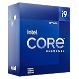
- Built for the Next Generation of Gaming. Game and multitask without compromise powered by Intel’s performance hybrid architecture on an unlocked processor.
- Discrete graphics required
- Compatible with Intel 600 series and 700 series chipset-based motherboards
- The processor features Socket LGA-1700 socket for installation on the PCB
- 30 MB of L3 cache memory provides excellent hit rate in short access time enabling improved system performance
This lets a design combine dies optimized for different functions, process nodes or manufacturing sources. A product team might separate high-performance compute from I/O, cache, analog circuitry or other supporting functions rather than building one enormous monolithic die.
Potential architectural advantages
- Shorter die-to-die connections can support higher bandwidth or lower communication energy.
- Different process technologies can be assigned to the functions that benefit from them most.
- Smaller chiplets may offer better manufacturing economics than one very large die, although package complexity adds its own yield risks.
- Validated tiles can potentially be reused across product families.
- Vertical integration can increase package-level capability beyond the practical size of a single lithography reticle.
These are architectural possibilities, not guaranteed gains for every product. Thermal removal, known-good-die screening, bonding defects and package-level testing become more demanding as stacks grow more complex.
Foveros versus EMIB
| Technology | Primary geometry | Role |
|---|---|---|
| Foveros | Vertical, 3D stacking | Places dies or compute tiles on top of a base die or package foundation. |
| EMIB | Horizontal, 2.5D connection | Uses embedded silicon bridges in the package substrate to connect adjacent dies. |
They are complementary, not synonyms. Intel can combine vertical Foveros stacks with horizontal EMIB connections in one heterogeneous package. Intel’s 2026 materials describe Foveros alongside EMIB and EMIB-T for scaling large AI-oriented packages.
Why Intel built the site in New Mexico
Rio Rancho already had semiconductor manufacturing and advanced-technology infrastructure. Expanding that campus allowed Intel to add packaging capacity, upgrade Fab 11X and co-locate related operations rather than creating an entirely separate U.S. site.
Do these 3 things before closing this tab:
1Repair Windows errors before they cause bigger problems2Fix the driver behind crashes, sound loss and screen glitches3Clear out junk files and repair common Windows errorsRank #3

- Game Without Compromise. Play harder and work smarter with Intel Core 14th Gen processors
- 20 cores (8 P-cores plus 12 E-cores) and 28 threads. Integrated Intel UHD Graphics 770 included
- Up to 5.6 GHz with Turbo Boost Max Technology 3.0 gives you smooth game play, high frame rates, and rapid responsiveness
- Compatible with Intel 600-series (with potential BIOS update) or 700-series chipset-based motherboards
- DDR4 and DDR5 platform support cuts your load times and gives you the space to run the most demanding games
Intel presents the New Mexico investment as supporting domestic manufacturing, high-tech employment, supply-chain resilience and foundry customers. Its investment materials are at Intel’s New Mexico investment page and its fact sheet is available as a PDF.
Those strategic goals should be separated from operating proof. Publicly available materials do not establish Fab 9’s utilization, annual capacity, product-by-product volumes, yields, revenue or profitability.
What Fab 9 means for Intel Foundry
For Intel Foundry, packaging expands the offer beyond wafer fabrication. A customer may need process technology, chiplet integration, package design, die-to-die interconnect, assembly, testing and qualification as one coordinated service.
Intel’s advanced-packaging overview presents support for 2D, 2.5D and 3D architectures and customer-oriented assembly and test. A domestic, co-located operation can make logistics and qualification easier for customers that want U.S.-based manufacturing.
Free tools Windows power users keep installed
One-click scans. No signup required.
Rank #4

- 10 cores (6 P-cores plus 4 E-cores) and 16 threads
- Performance hybrid architecture integrates two core microarchitectures, prioritizing and distributing workloads to optimize performance
- Up to 4.7 GHz unlocked. 20MB Cache
- Compatible with Intel 600-series (with potential BIOS update) and 700-series chipset-based motherboards
- PCIe 5.0 and 4.0 support. DDR4 and DDR5 Memory support. RM1 thermal solution included. Discrete graphics required.
Opening Fab 9 alone does not demonstrate that Intel Foundry has won large external customers or achieved a particular margin. Customer names, production volumes and financial outcomes should be treated as established only when Intel or the customer discloses them.
What has been demonstrated—and what remains unknown
Established by Intel’s public announcements
- Fab 9 is in Rio Rancho, New Mexico.
- Intel celebrated its opening on January 24, 2024.
- The facility supports high-volume advanced semiconductor packaging, including Foveros.
- Fab 9 and Fab 11X form a co-located advanced-packaging operation.
- Intel continues to identify the site as an active Foveros facility in its July 29, 2026 coverage.
Not disclosed in the cited public materials
- Fab 9’s exact annual capacity or utilization rate.
- Customer-specific production volumes and a complete product list.
- Fab 9-specific yield, revenue or profit.
- Whether every current Foveros variant is produced at this site.
Intel’s 2026 article reports that the broader New Mexico operation has grown to 2,700 employees and 500 suppliers. That is a site-level figure, not Fab 9-only employment. Intel’s current account of the operation is at Intel’s U.S. advanced-packaging overview.
Independent reader supportYour contribution helps us test, update, and keep practical guides available for everyone.Why the 2024 milestone still matters in 2026
Intel has said Foveros has been in mass production since 2019; Fab 9 therefore was not the first appearance of Foveros in any form. Its significance was establishing a major U.S. high-volume operational site dedicated to advanced package integration.
That matters as AI and high-performance-computing systems increasingly use multiple specialized dies. Packaging can become a competitive foundry product because customers may value a supplier that coordinates wafers, chiplets, interconnects, assembly and testing. The same model also brings trade-offs: more complex thermal design, tighter known-good-die requirements, additional inspection and bonding costs, and greater dependence on compatible design tools and qualification procedures.
Best Value
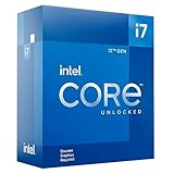
- Intel Core i7 3.60 GHz processor offers more cache space and the hyper-threading architecture delivers high performance for demanding applications with better onboard graphics and faster turbo boost
- The Socket LGA-1700 socket allows processor to be placed on the PCB without soldering
- 11 MB L2 and 25 MB L3 cache offers supreme performance for computation intensive apps
- Intel 7 Architecture enables improved performance per watt and micro architecture makes it power-efficient
The company’s U.S. manufacturing and CHIPS Act overview places New Mexico within Intel’s broader domestic-manufacturing strategy. That policy context does not, by itself, establish Fab 9’s commercial performance.
Bottom line for investors and supply-chain analysts
“Fab 9 starts operations” is a 2024 milestone, not a new 2026 opening. Fab 9 is an advanced-packaging facility, not a leading-edge processor fab. Its enduring importance is the combination of high-volume Foveros 3D integration, co-location with Fab 11X and a U.S. manufacturing base that supports Intel’s attempt to sell packaging as part of an end-to-end foundry service.
For a broader view of Intel’s Foveros variants and roadmap disclosures, see the company’s 2025 Form 10-K. The filing does not turn the Fab 9 opening into evidence of specific utilization, customer volume or profitability.
Quick Recap
Product prices and availability are accurate as of the date/time indicated and are subject to change. Any price and availability information displayed on Amazon at the time of purchase will apply.




